rp417 — RP2354B × CH32H417, automated limit testing
An open-hardware board (KiCad) on which a Raspberry Pi RP2354B (RP2350 family) supervises a WCH CH32H417MEU6. The RP2354B powers, resets, programs, stimulates and measures the CH32 so that a PC script can run automated limit tests on it: USB3 throughput, parallel ADC capture (DVP), the CH32’s internal ADC and HSADC, and microSD (SDIO). Both chips have their own USB port to the host, and the board also works with no host on the RP2354B’s USB.
Status: v1.0 (rev A) — schematic complete, PCB fully routed by hand (6 layers, 63.5 × 88.9 mm, 0 unconnected), JLCPCB production files generated with an LCSC number on every BOM line. Not fabricated yet; no firmware yet. Source on GitHub.
| Top | Bottom |
|---|---|
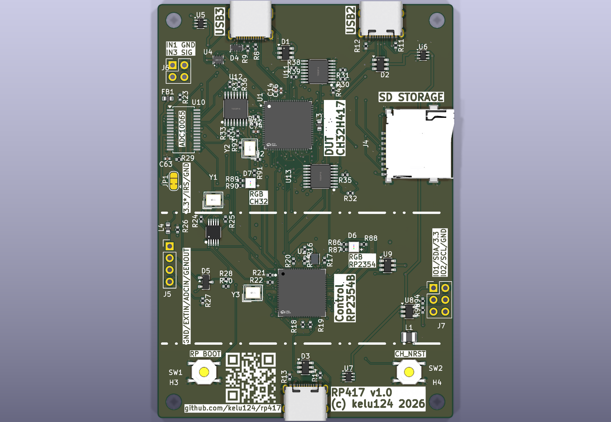 |
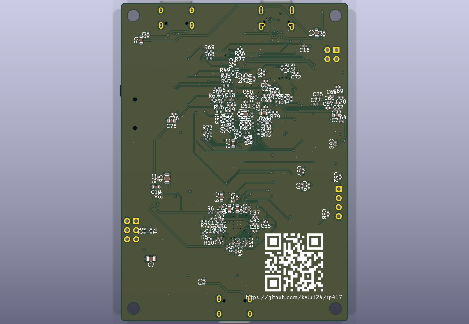 |
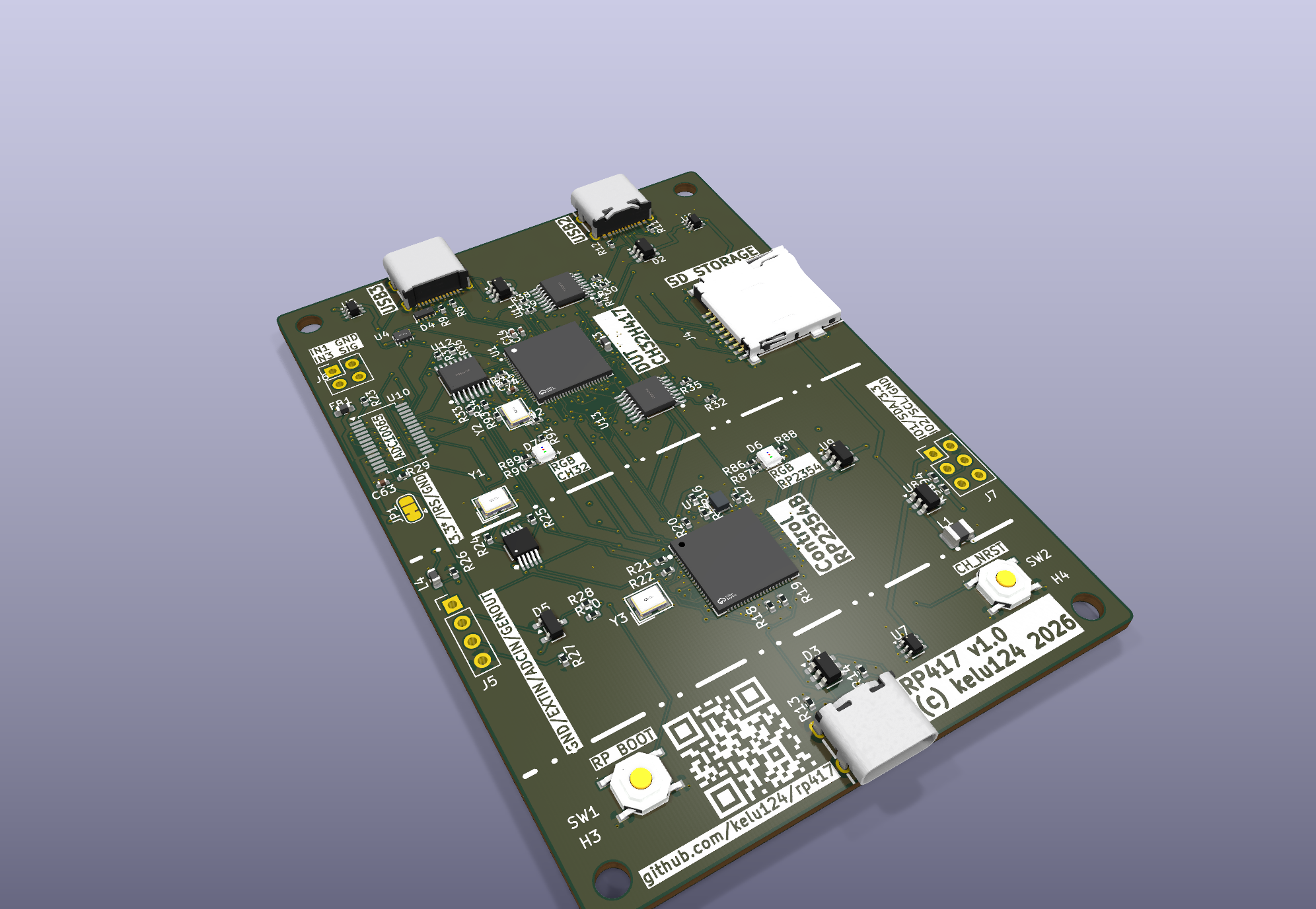
What it does
| Block | RP2354B (supervisor) | CH32H417MEU6 (device under test) |
|---|---|---|
| USB | USB 2.0 on USB-C J3 (test control, CH32 programmer) | USB3 SuperSpeed + USB2 HS on USB-C J1; USB FS on USB-C J2 (also USB ISP) |
| Storage | 2 MB flash in the package | microSD J4 on SDIO/SDMMC |
| Capture | 10-bit PIO counter pattern into the CH32 DVP (lost / duplicated sample check) | DVP 10-bit capture of an ADC10065 (65 MSPS) or of the RP counter |
| Analog | Si5351A clock + test-signal generator (5th-order LC filter, ≈ 28.6 MHz corner) | 12-bit ADC + 10-bit HSADC fed from the same stimulus; HSADC test header J6 |
| User I/O | RGB LED, BOOTSEL button, SAO header J7 (I2C0) | RGB LED, RESET button |
| Control | switches the CH32 power, drives NRST, selects the capture source and the USB/debug switch | — |
- Inter-chip links: UART, I2C, QSPI (CH32 master, RP PIO slave), an 8-line GPIO logic bus, HSYNC/VSYNC and a shot marker — every line with a series resistor.
- Programming: the RP2354B is a ch32fun / minichlink “funprog” programmer on the CH32’s SDI pins (PB8/PB9, shared with USB HS through a TS3USB221A switch). Fallback: the CH32 bootloader, entered by power-cycling it.
- Power: any of the three USB-C ports powers the whole board (3 × LM66100 ideal diodes); one always-on 3V3 buck; the CH32 domain sits behind an RP-controlled load switch.
Documentation
| Page | Content |
|---|---|
| Architecture | Blocks, inter-chip links, programming, capture path, standalone mode |
| Pin map | Every RP2354B ↔ CH32 link and every pin of both chips (generated from the netlist) |
| Power | Power paths, ideal-diode ORing, CH32 load switch, rails, back-feed protection |
| Layout and routing | How the KiCad files are generated, stack-up, placement, plane fan-out, routing |
| Bill of materials | JLCPCB parts with LCSC numbers, consigned and DNP parts |
| Production | Ordering at JLCPCB: files, settings, checklist |
| Images | 3D renders, copper layer plots, assembly views |
| CH32H417 hardware notes | Facts from the CH32H417 datasheet and reference manual that shaped the design |
| Design page | Original block diagrams, pin plans, parts list and area budget (rev A design phase) |
Requirements and design decisions (R1–R10, D01–D69) are in
.claude/SPEC.md and
.claude/DECISIONS.md.
Downloads
| File | |
|---|---|
| rp417.zip | Gerbers + drill files (JLCPCB) |
| bom.csv | Assembly BOM with LCSC part numbers |
| positions.csv | Assembly placement (CPL) |
| KiCad board | Routed v1.0 board (KiCad 10) |
| KiCad schematic | Generated schematic (root sheet + 6 sub-sheets) |
How the design is made
The schematic is generated from one Python file, hw/gen/build.py (parts, footprints, LCSC numbers, pin→net map).
hw/gen/pcb.py places the parts (passives perpendicular to their IC pin) and fans power pads out to the planes;
Freerouting gave a first draft, and the board was then routed by hand in KiCad. hw/gen/gen_site.py regenerates
this site’s images, pin map and BOM page. Details: Layout and routing.
References
- CH32H417 datasheet and reference manual (WCH);
markdown copies in
datasheets/. - ch32fun — minichlink and the funprog programmer core.
- RP2350 datasheet and hardware design guide.
- Freerouting, easyeda2kicad.
- Sister project: rp569 (RP2350B × CH569, USB 3.0 for PIO).
License
Copyright Luc Jonveaux 2026. Hardware: TAPR Open Hardware License; software: GPL v3 or later; docs: CC BY-SA 3.0 — same terms as rp569 and pic0rick.