Layout and routing
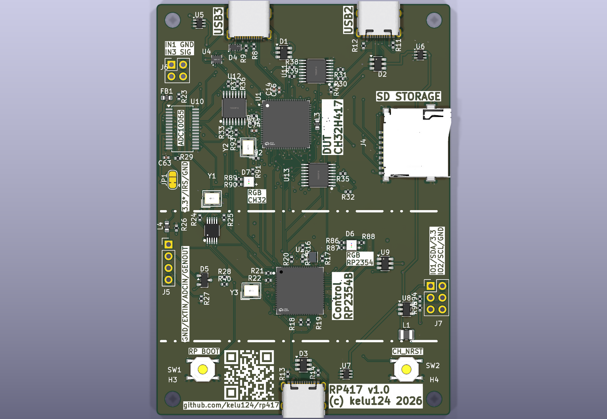
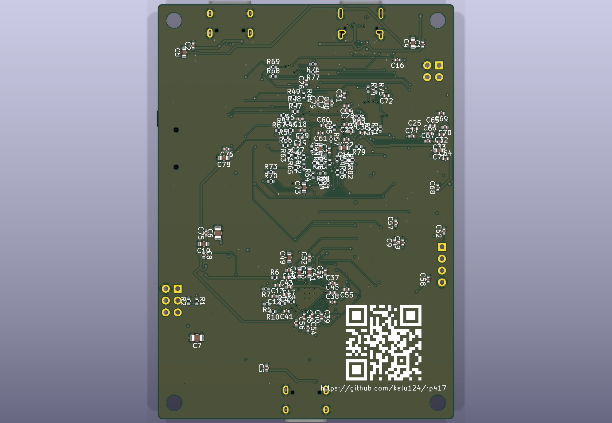
Status: v1.0 (rev A), 2026-11-14 — fully routed by hand, 0 unconnected. Remaining DRC items are known and reviewed: 21 waived errors inside the USB-C connector footprints (D59), silkscreen flags from the QR codes, and 23 starved thermal reliefs to review before ordering.
| Top | Bottom |
|---|---|
 |
 |
Board
- 6 layers, 63.5 × 88.9 mm (playing-card size, D19), JLCPCB fab and assembly (D18).
- Parts on both sides (D48): connectors, ICs, crystals, analog and ESD on top; decoupling, series-R groups, bias networks, ideal diodes and the load switch on the bottom.
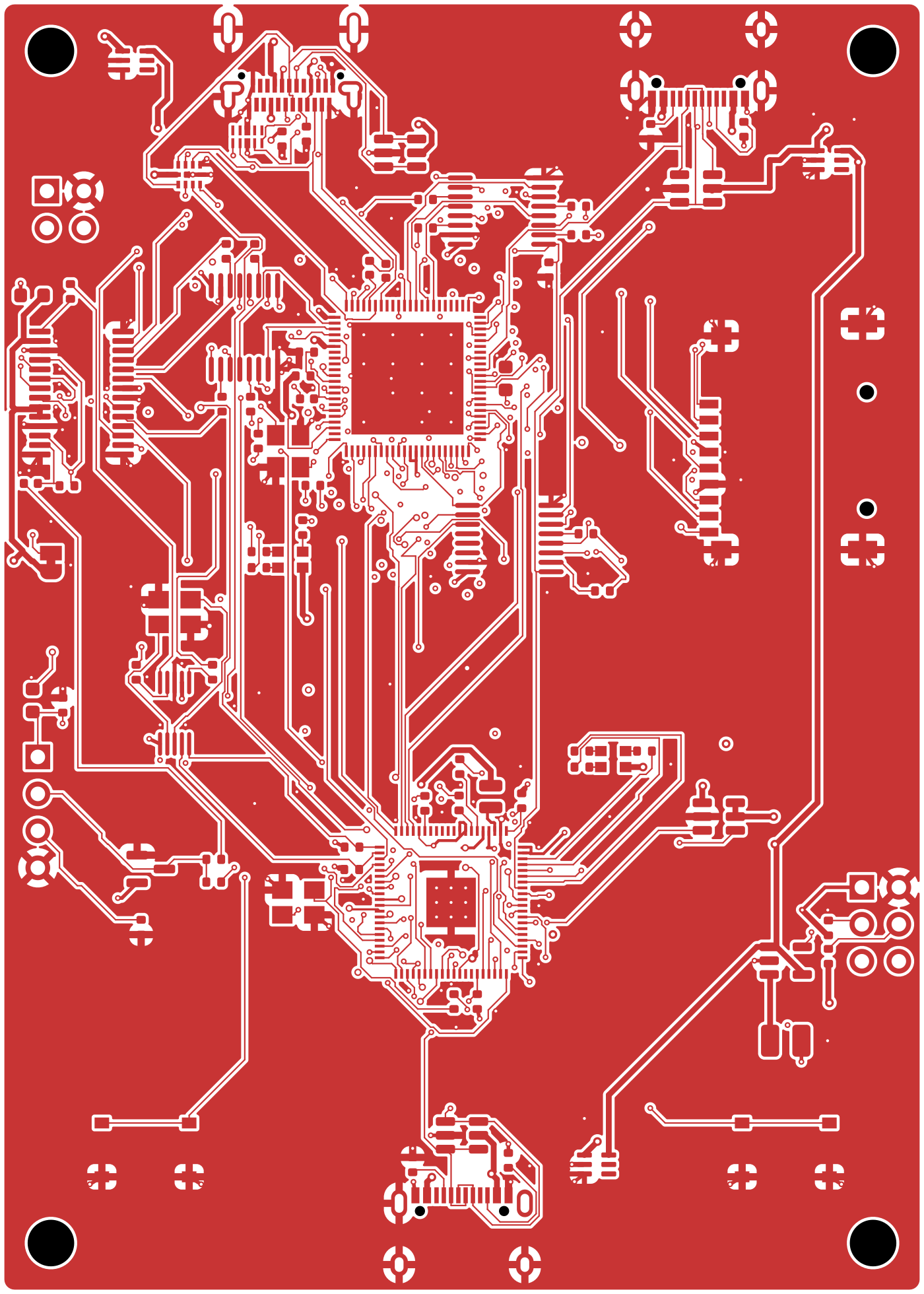
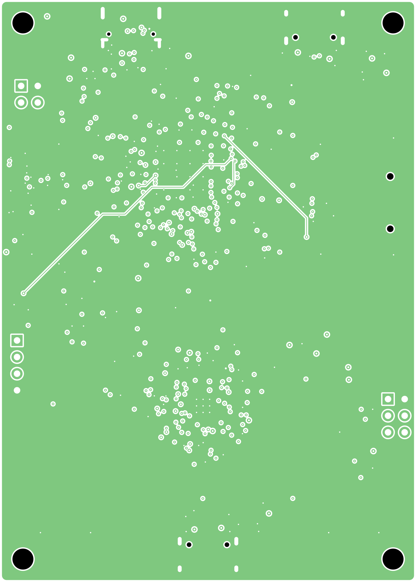
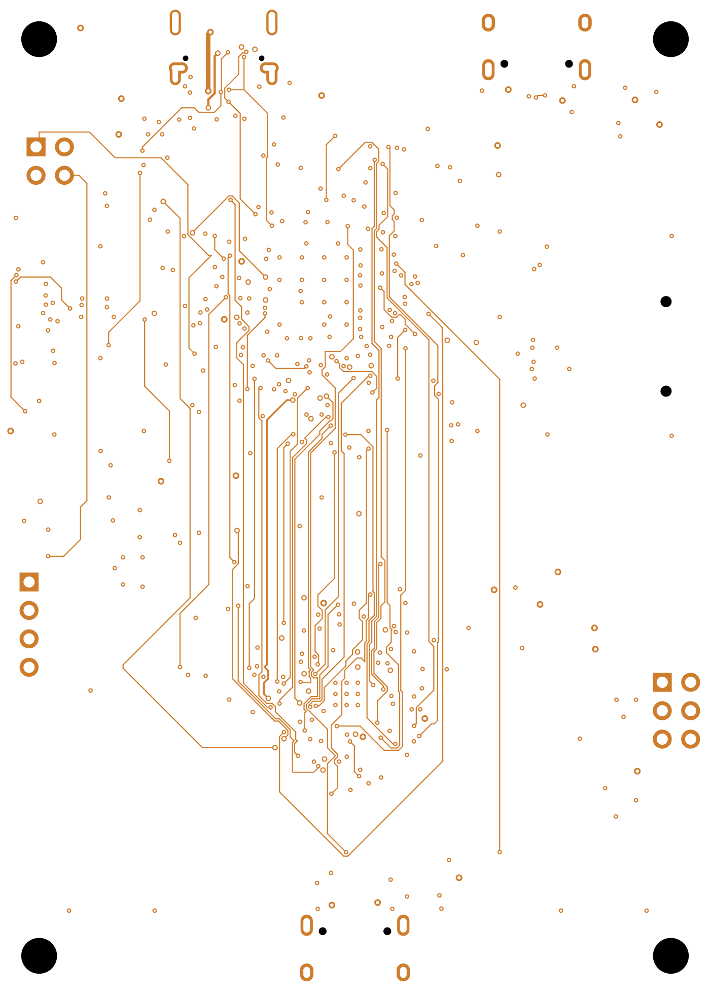
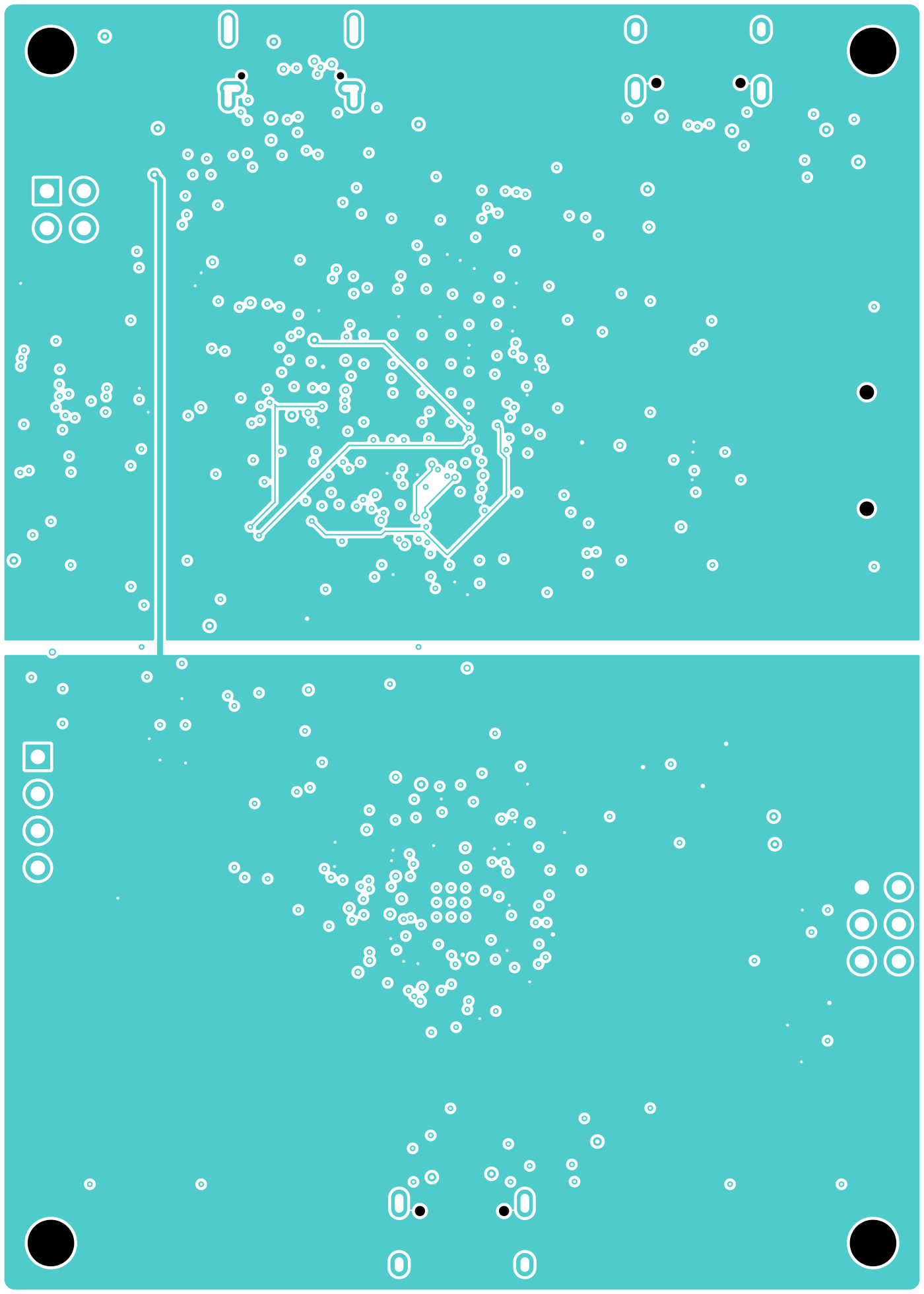
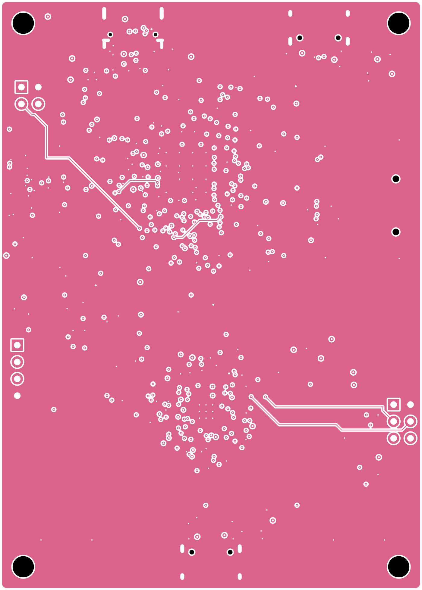
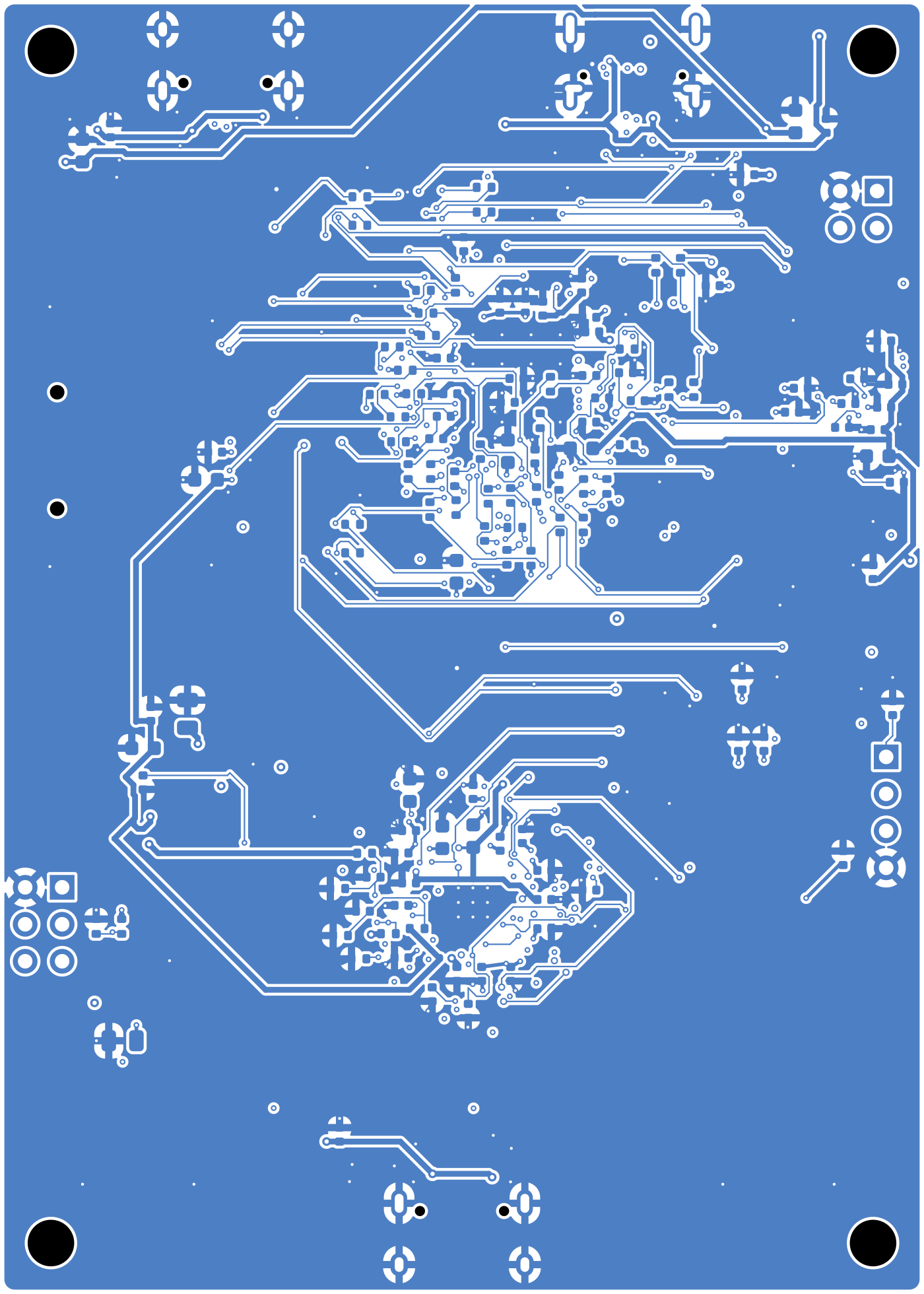
- Stack-up: F.Cu signal · In1 GND · In2 signal · In3 power (+3V3_CH top / +3V3 bottom) · In4 GND · B.Cu signal.
- Net classes: Default 0.1 mm track / 0.1 mm clearance, via 0.4/0.2 mm; Power 0.4 mm.
How the KiCad files are produced
| Script | Output |
|---|---|
hw/gen/build.py |
Netlist source of truth: every part, value, footprint, LCSC number and net → the schematic (root + 6 sheets) and nets.json |
hw/gen/kisch.py |
Minimal schematic writer: each pin gets a stub and a global label (a netlist, not a drawing) |
hw/gen/pcb.py |
Footprints, placement, zones, plane fan-out → hw/build/rp417_placed.kicad_pcb + a Specctra DSN |
hw/gen/finish.py |
Imports a Freerouting session, fills zones, runs DRC (never overwrites the hand-routed board, D61) |
hw/gen/gen_site.py |
This site’s images, pin map and BOM page |
Late changes after hand routing started (LEDs, test headers, SAO header) were added at the end of build.py, so
no existing reference is renumbered, and placed directly in the routed board.
Placement rules
- Fixed anchors for connectors, ICs and crystals; the CH32 sits near J1 (USB3), the RP2354B in the lower half.
- Passives tied to an IC pin are placed perpendicular to that IC edge, with the IC-side pad facing the pin (D53); decoupling capacitors one per power pin, on the bottom under or next to it.
- Capture switches next to their DVP pin groups (D57): U11 top edge, U12 left edge, U13 bottom edge of the CH32.
Plane fan-out (D60)
Generated before routing: a locked 0.4/0.2 mm via with a 0.25 mm stub (“dogbone”) on every SMD pad of GND, +3V3 and +3V3_CH, placed away from the nearest QFN; a 4 × 4 via grid in the CH32 exposed pad and 3 × 3 in the RP2354B pad; the QFN power pins reach their plane through their decoupling capacitor.
Routing
- Freerouting 2.1.0 gave a first draft (60 → 26 open connections after the fan-out). Gotcha: headless, it
ignores
-mp/--router.max_passesand only saves its session when it finishes — use--router.job_timeoutto stop it cleanly (details inhw/README.md). - Hand routing in KiCad finished the board (D61), including the late additions.
Things the autorouter could not control and that were reviewed by hand: the USB3 SuperSpeed pairs (J1 ↔ CH32), the USB HS/FS pairs, the crystals, PCLK and the DVP bus.
Copper layers
| F.Cu | In1 (GND) | In2 (signal) |
|---|---|---|
 |
 |
 |
| In3 (+3V3_CH / +3V3) | In4 (GND) | B.Cu (seen from below) |
|---|---|---|
 |
 |
 |
3D models
The LCSC parts use the manufacturers’ models fetched with easyeda2kicad (D67): .wrl files committed in
hw/lib/lcsc.3dshapes/, .step files gitignored (refetch command in hw/README.md).