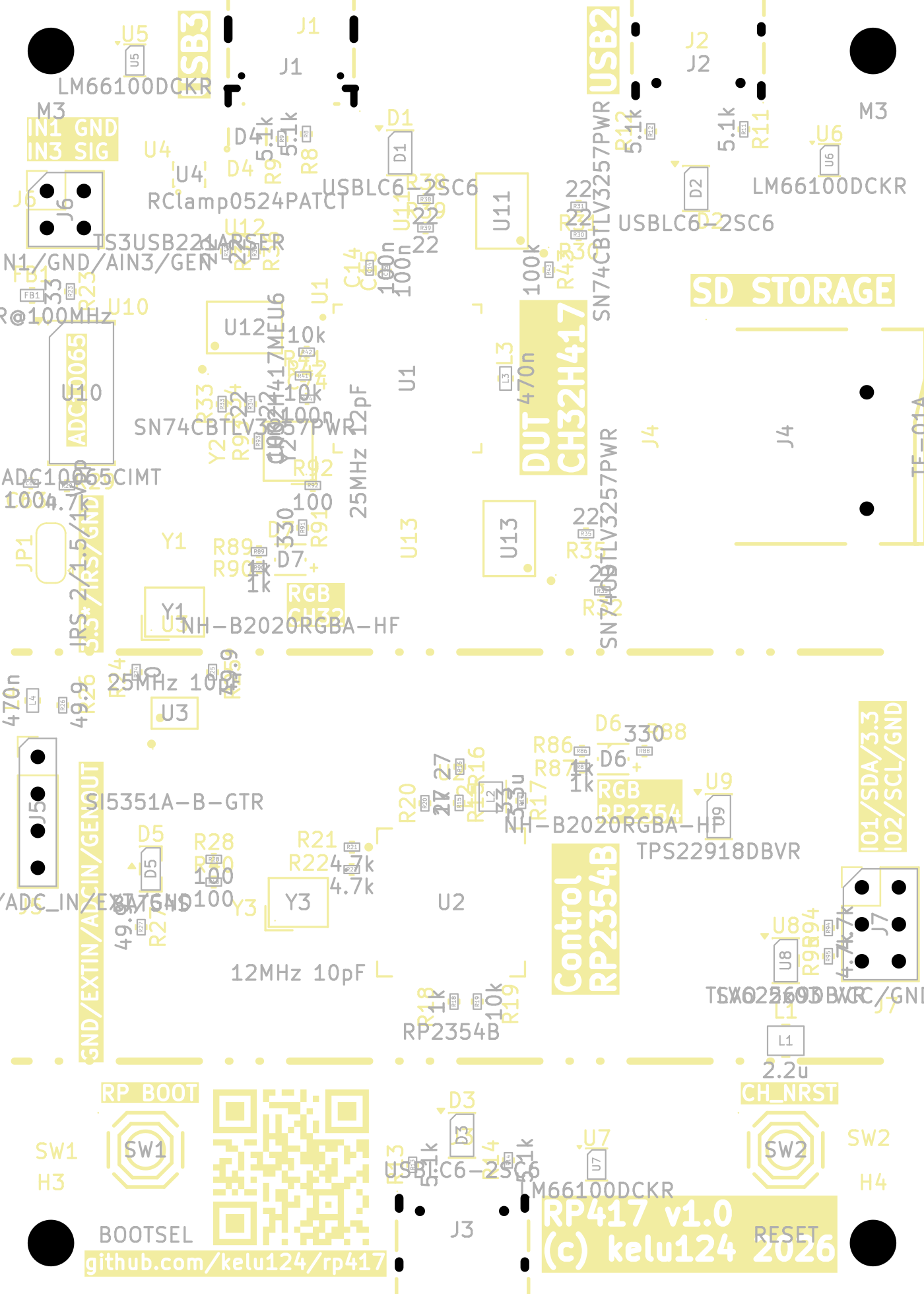
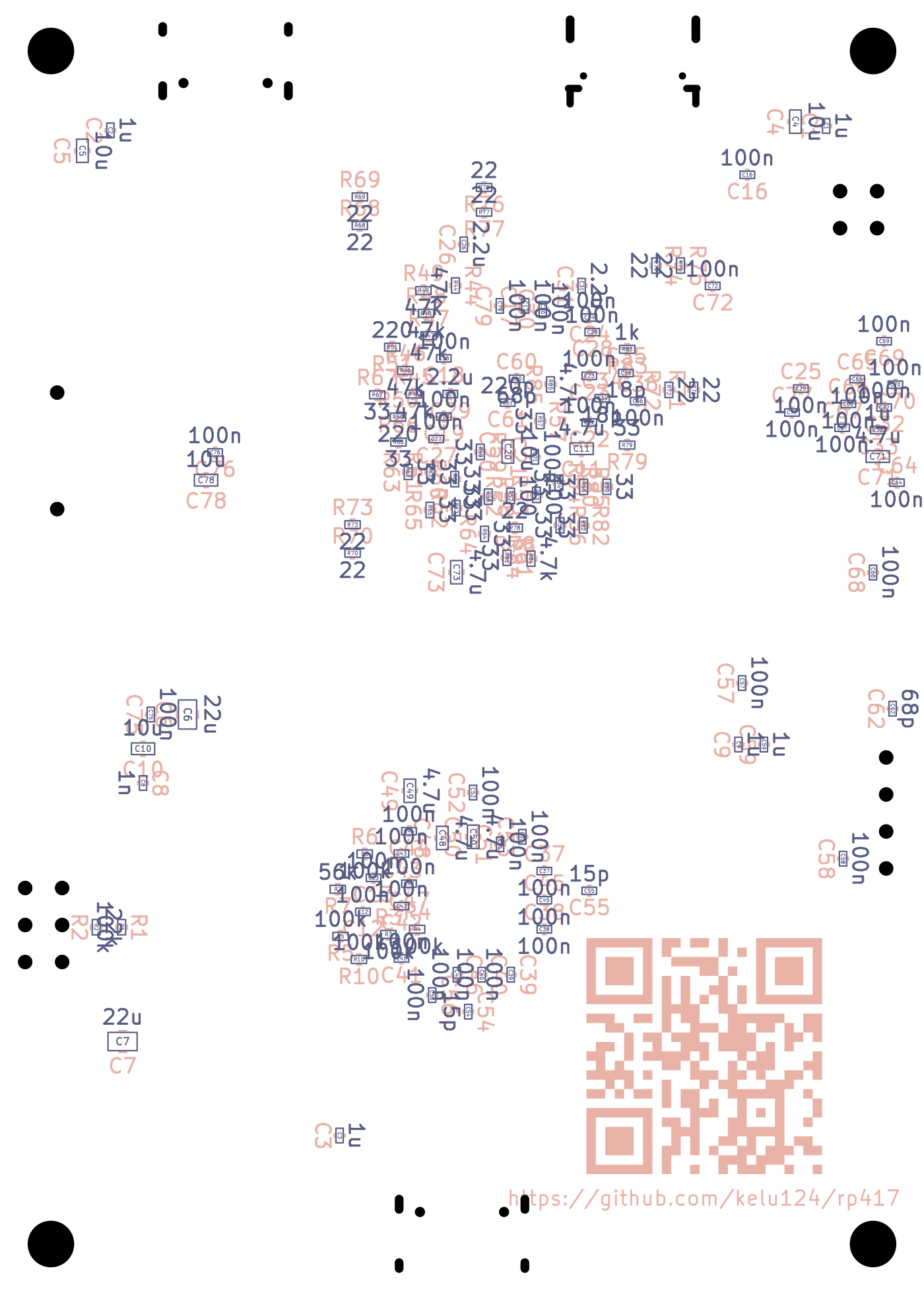
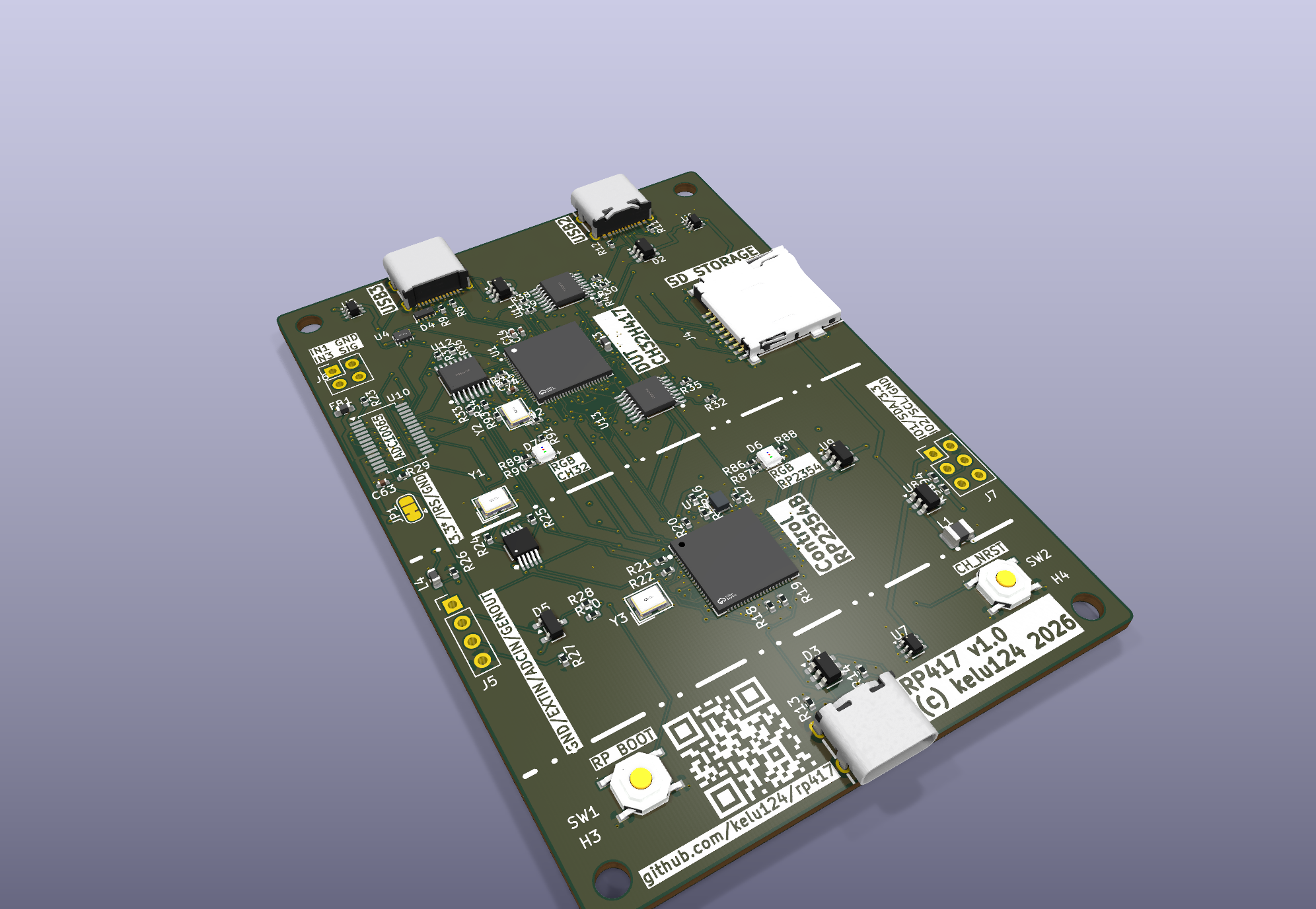
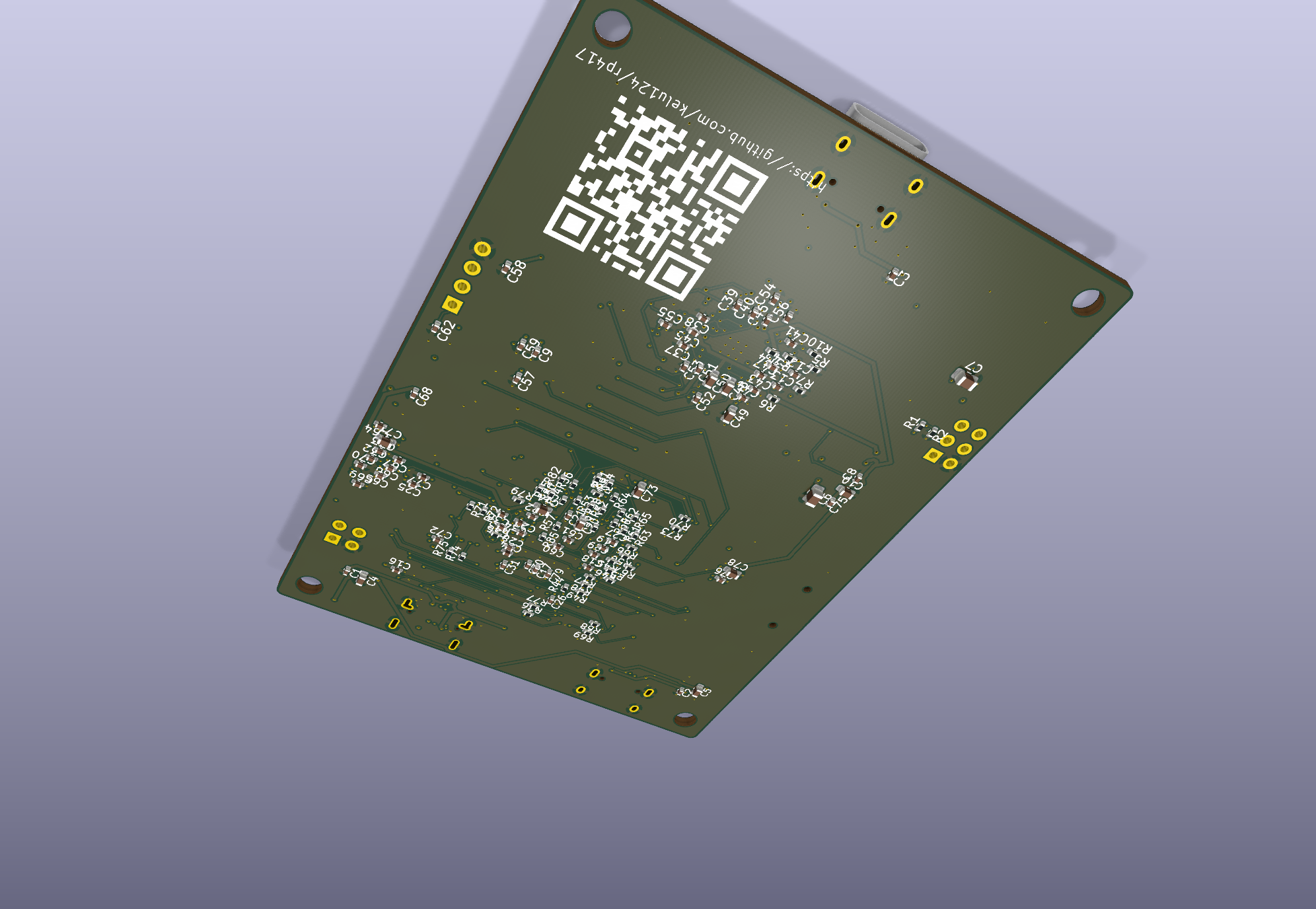
Board images (v1.0)
Renders from kicad-cli pcb render of hw/rp417.kicad_pcb (commands in hw/README.md); layer plots and assembly
views written by /usr/bin/python3 hw/gen/gen_site.py (re-run after board changes).
| Top | Bottom |
|---|---|
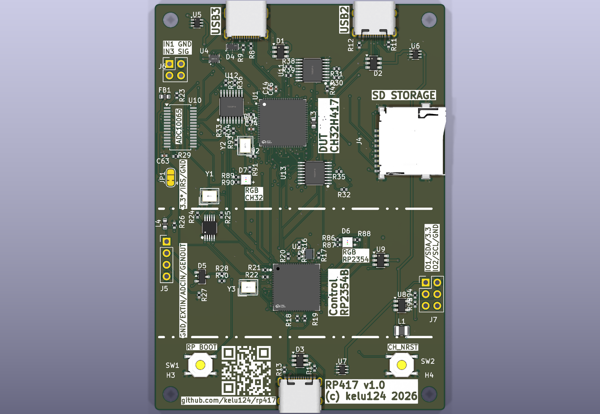 |
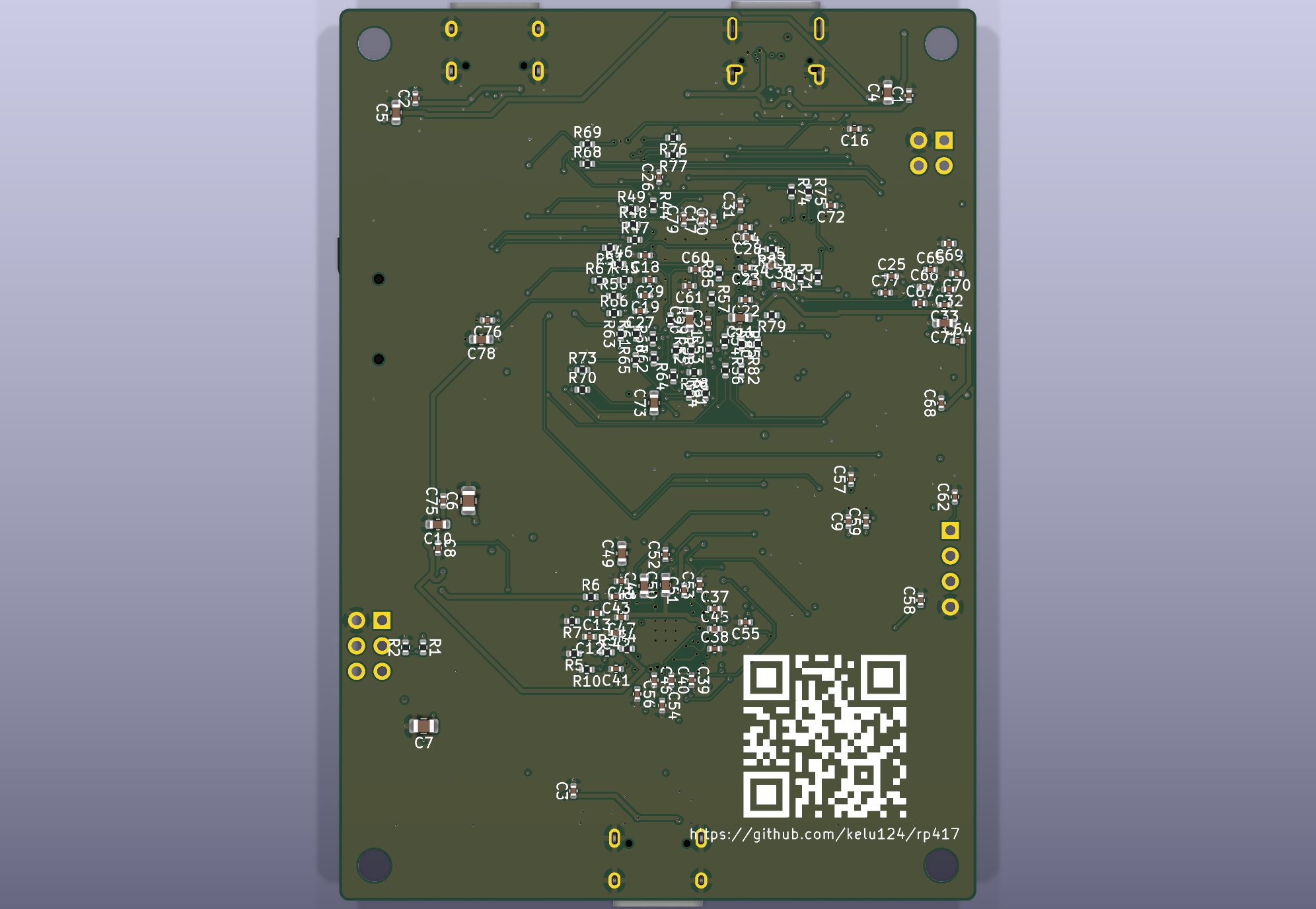 |
 |
 |
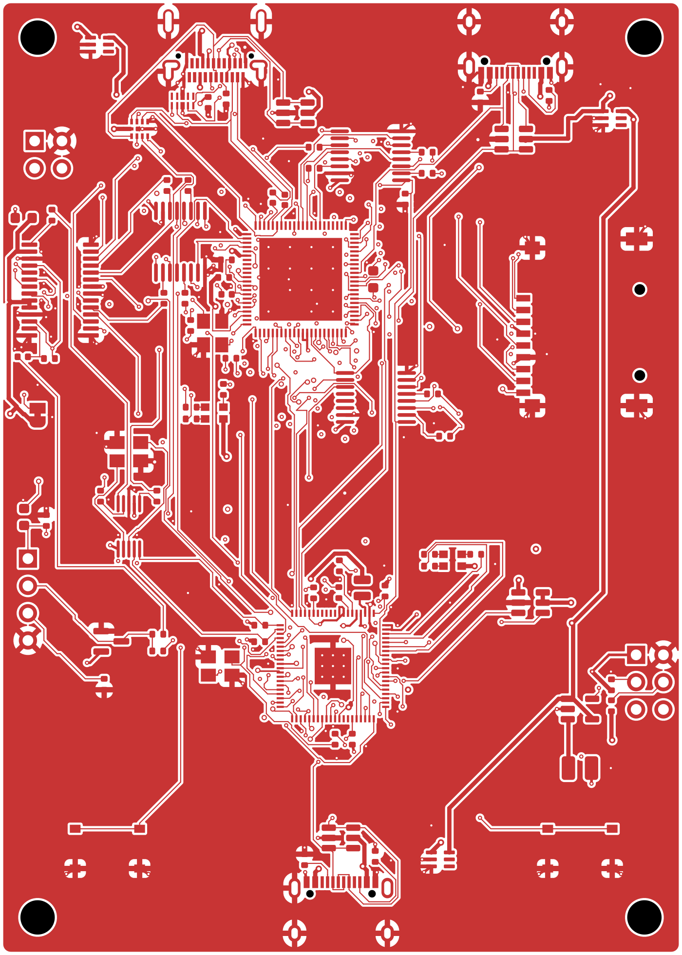
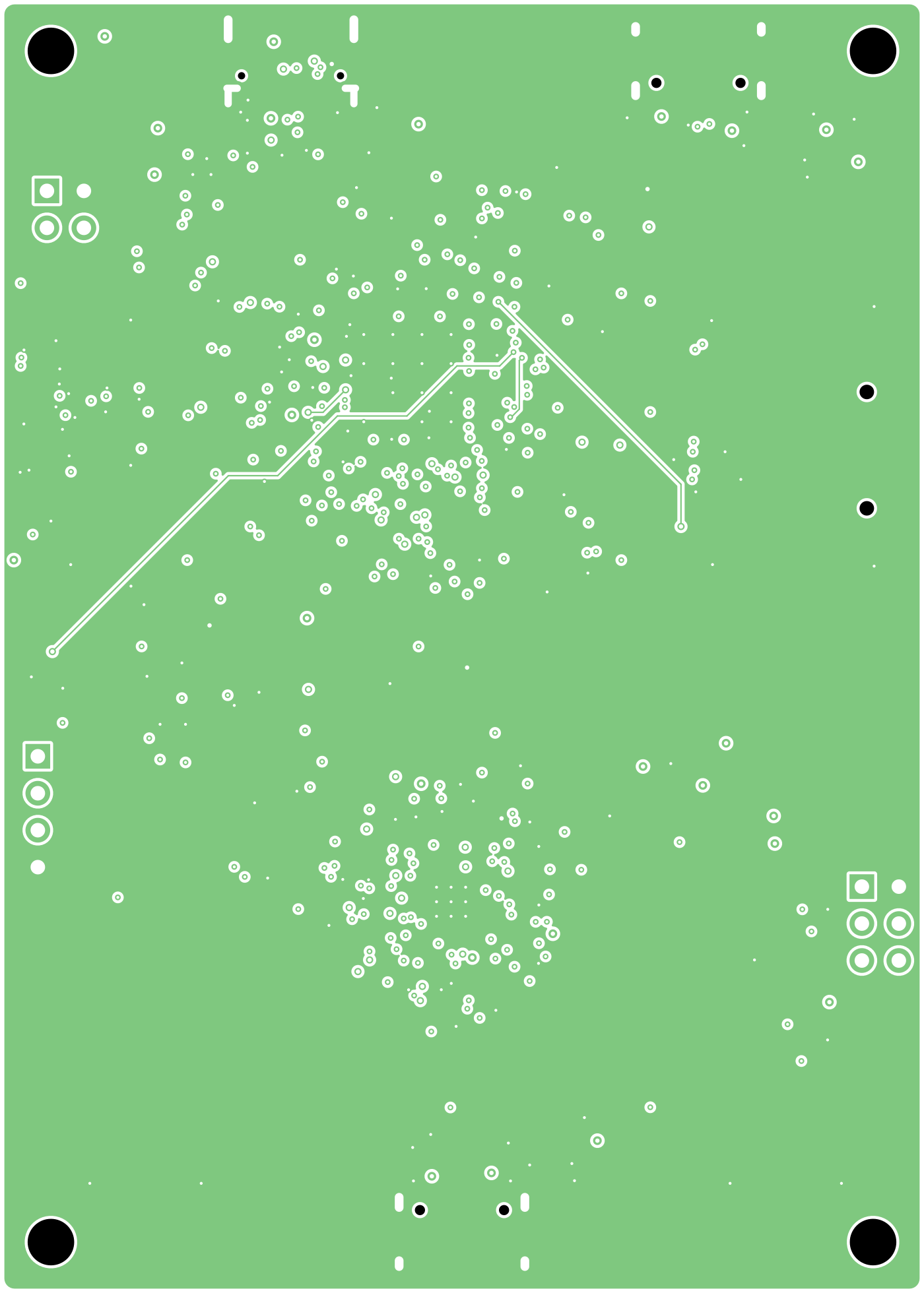
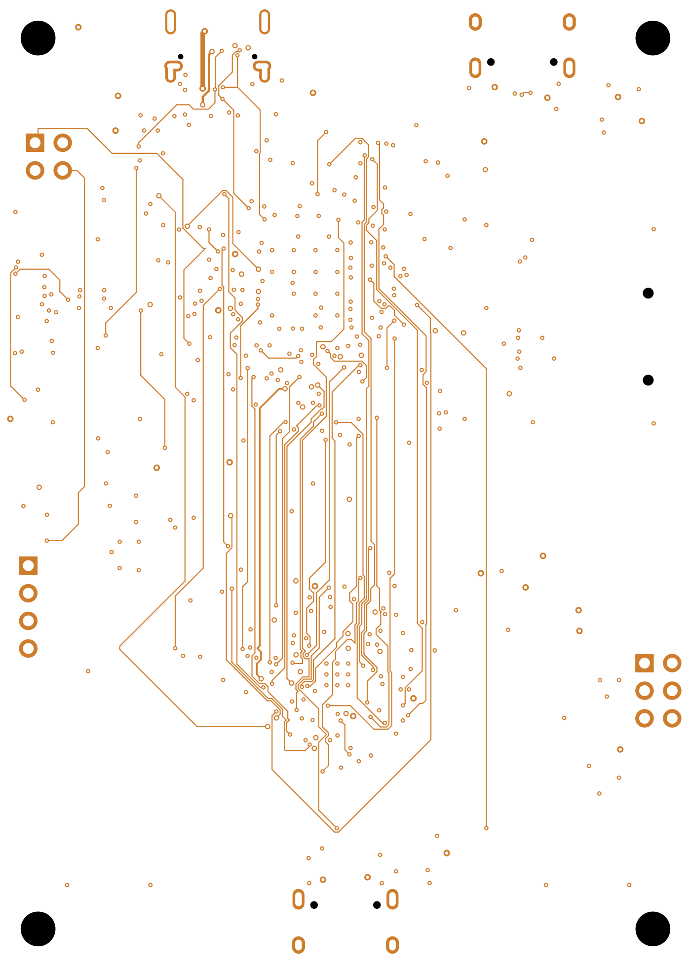
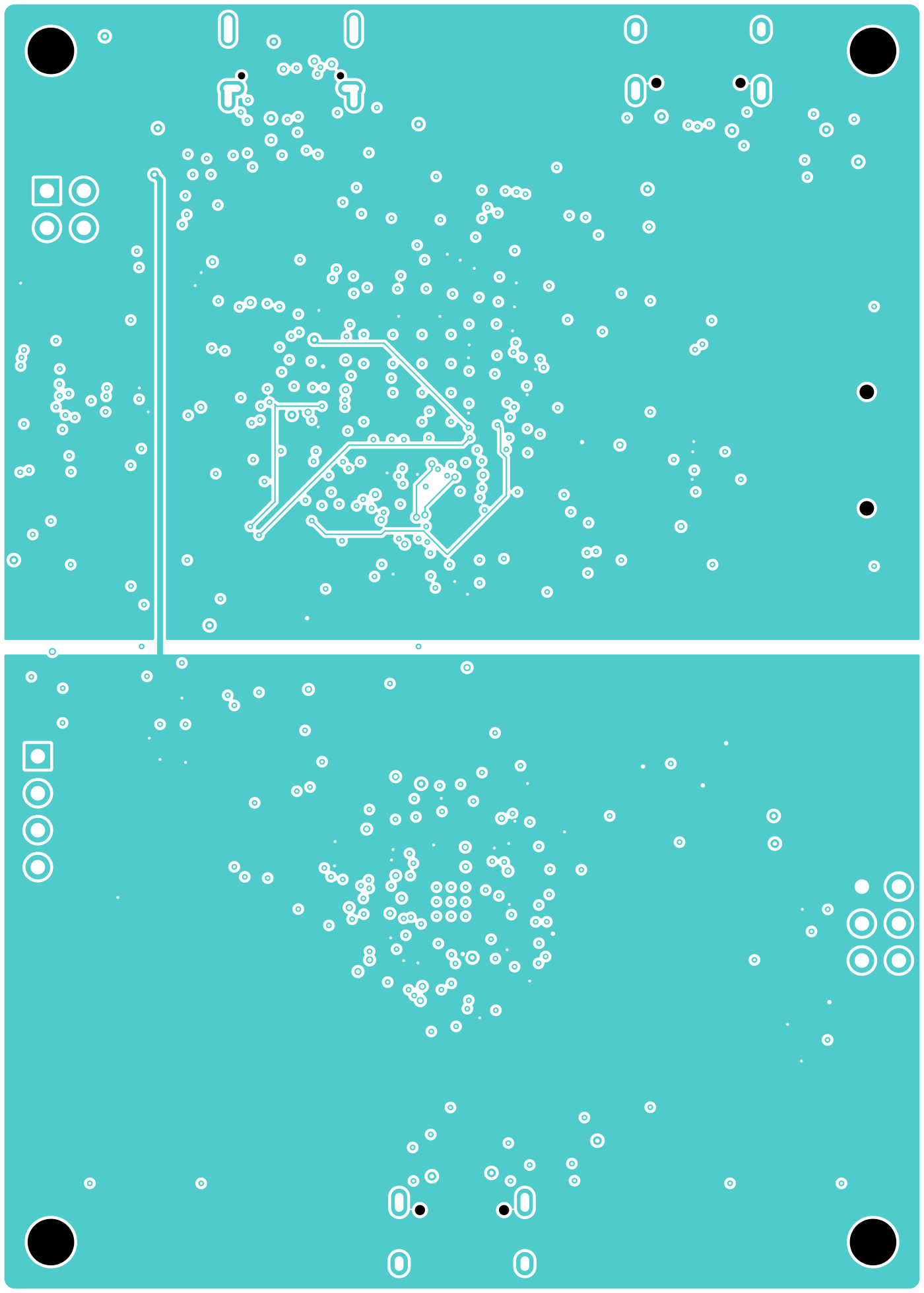
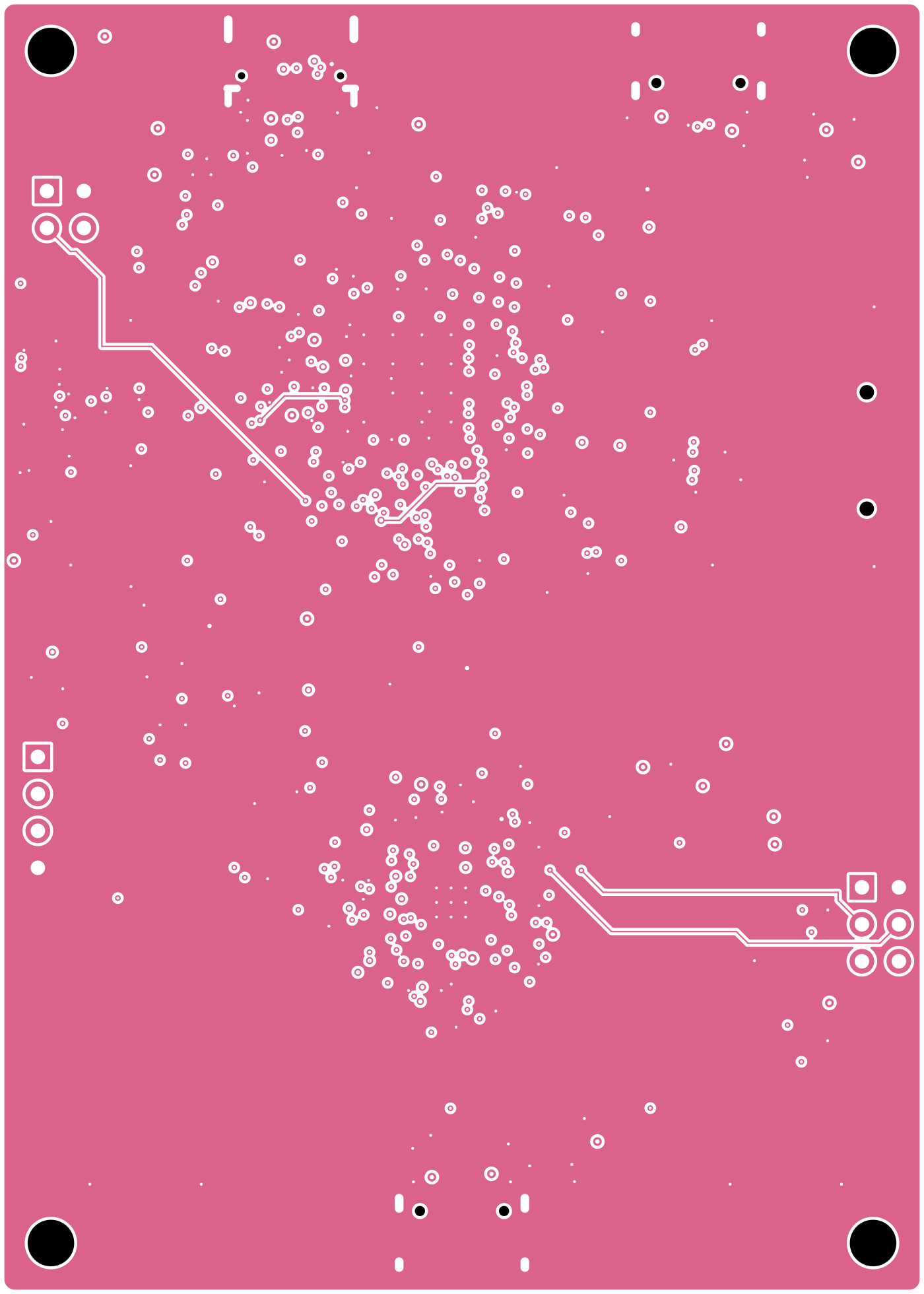
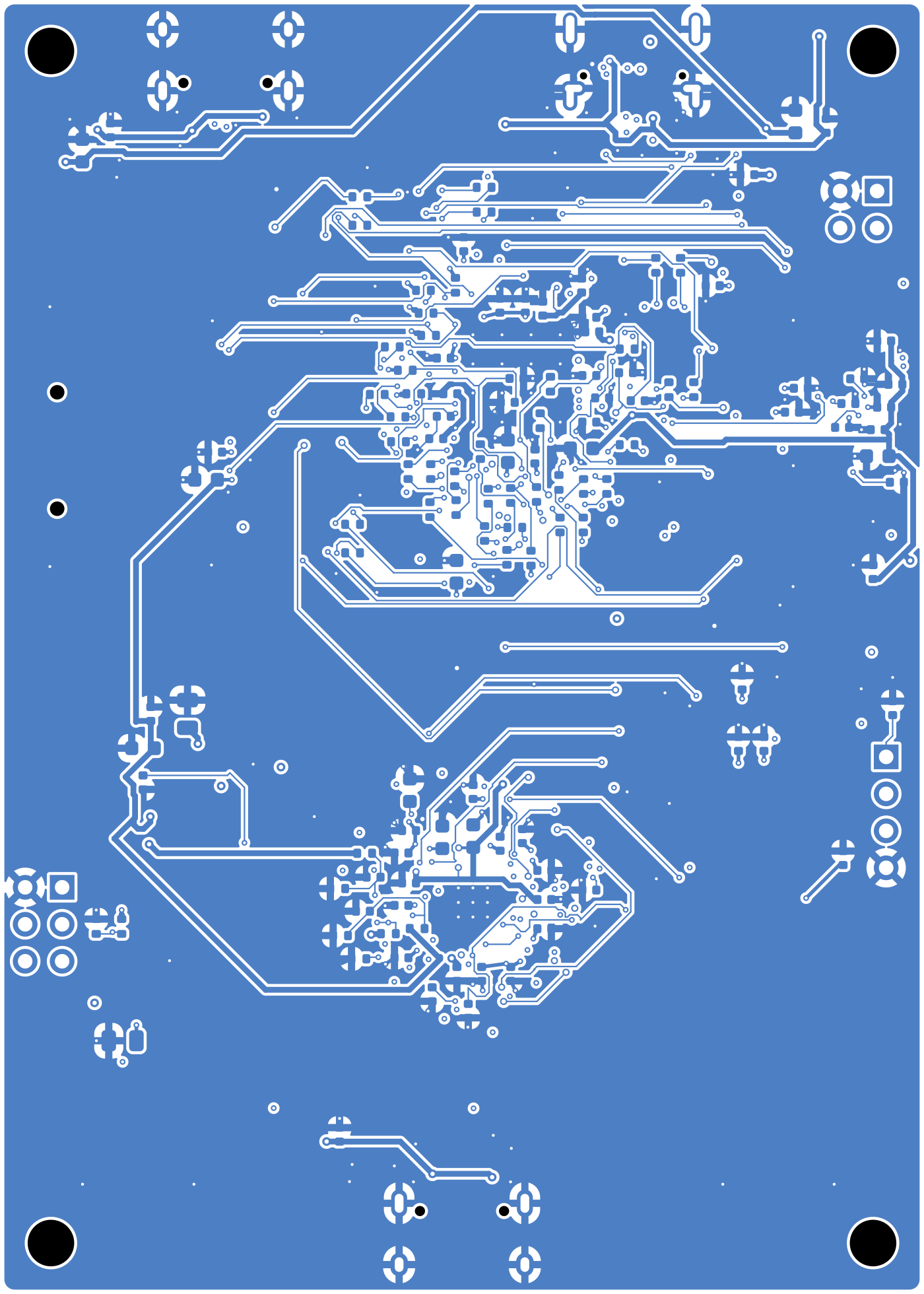
Copper layers (board area; B.Cu mirrored as seen from below):
| F.Cu | In1 (GND) | In2 (signal) |
|---|---|---|
 |
 |
 |
| In3 (+3V3_CH / +3V3) | In4 (GND) | B.Cu |
|---|---|---|
 |
 |
 |