Layout status
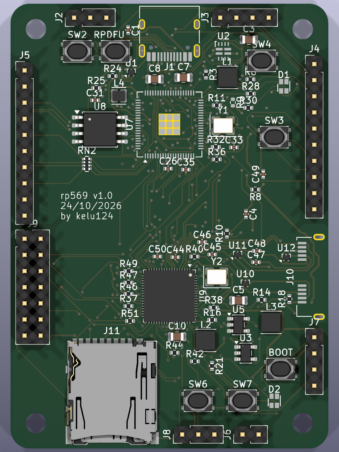
Status: v0.3, 2026-10-24. Schematic complete, PCB placed (50×70 mm, two-sided). v1.0 board:
hardware/rp569-routed.kicad_pcb — KRT autoroute finished by hand, 0 unconnected, 0 DRC errors (D-021:
some tracks on In1). Production files in hardware/jlcpcb/ (D-022). Still to do before ordering: USB pairs as
coupled pairs, silkscreen; see .claude/todo.md.
| Top | Bottom |
|---|---|
 |
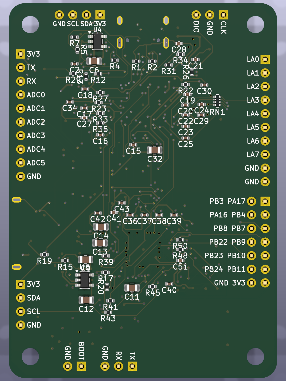 |
(v1.0, kicad-cli pcb render of hardware/rp569-routed.kicad_pcb)
How the KiCad files are produced
Everything under hardware/ is generated from hardware/gen/board.py (parts, footprints, pin→net map):
| Script | Output |
|---|---|
gen/mk_lib.py |
lib/rp569.kicad_sym: CH569W symbol from phantomdrive (MIT), pin types corrected; TPS2121 |
gen/mk_fp.py |
lib/rp569.pretty: GSB343K33HR and TI RUX0012A footprints from the datasheets |
gen/gen_sch.py |
rp569.kicad_sch: one sheet, symbols grouped by block, a net label on every pin |
gen/gen_pcb.py |
rp569.kicad_pcb: 4-layer 50×70 mm with 3 mm rounded corners, footprints + nets, fixed connectors/chips/buttons/LEDs, two-sided automatic placement, GND plane on In1 |
gen/gen_pro.py |
net classes in rp569.kicad_pro (USB3_90R, USB2_90R, HSPI, Power, Rail) |
gen/route_krt.sh |
KiCadRoutingTools chain on a copy of the board (Routing options B) |
gen/gen_fab.py |
DRC gate, then gerbers + drill (jlcpcb/rp569-gerbers.zip), BOM and CPL from rp569-routed.kicad_pcb |
gen/gen_bom.py |
JLCPCB BOM and CPL in hardware/jlcpcb/ |
gen/build.sh |
runs all of the above, then ERC and DRC with schematic parity → hardware/reports/ |
Once hand-routing starts, stop running gen_pcb.py: it rebuilds the board from scratch and would
wipe the routing. From then on, change board.py → gen_sch.py → in pcbnew Tools → Update PCB from
Schematic. Footprints are already linked to their symbols, and schematic parity is 0 issues.
Check results (v0.3)
- ERC: 0 errors. Schematic ↔ PCB parity: 0 issues.
- DRC (unrouted board): 0 electrical violations; ~100 silkscreen overlaps (cosmetic); 405 unrouted connections.
Placement summary (D-011, D-017, D-018)
Board 50×70 mm, portrait, 3 mm-radius rounded corners (D-023; 45° chamfers until then), M3 holes 4 mm from each corner.
- Chips (top side): RP2350B at (25, 19) rotated 90° so GPIO8–23 (HSPI) face down; CH569W at (25, 46) rotated 270° so its HSPI pins face up and its USB3 pins sit at its top-right corner. The HSPI bus runs straight between them (no series resistors, D-018).
- Connectors: USB-C top edge; USB3 Micro-B right edge (y 43); microSD bottom-left.
- Headers (THT): top edge SWD + RP I2C; left edge LA IN (1x10) + CH EXT (2x07); right edge RP EXT (1x10, with the RP debug UART) + CH I2C; bottom edge CH UART + CH BOOT JP.
- Buttons and LEDs at the edges, on their chip’s half (D-018): BOOTSEL/RUN top-left, RP BTN1/BTN2 and RP LED on the right of the RP2350 half, CH BTN1/BTN2, CH569 BOOT and CH LED bottom-right.
- Passives: placed by
gen_pcb.pynext to the pads they connect to, turned toward their net partners; decoupling caps prefer the bottom side under their IC; the bottom area under each QFN (pads + 1.2 mm) is kept free for vias. - Pins reassigned by chip side so each line leaves toward its destination (D-018,
docs/pinmap.md).
Rules (D-016, D-017)
JLCPCB JLC04161H-7628 4-layer stack. F.Cu / In2.Cu / B.Cu are routing layers, In1.Cu is the solid GND plane (reference for the 90 Ω USB pairs on F.Cu). Net classes: Default 0.15/0.1 mm, Rail 0.2/0.1 mm (+3V3, 3V3_CH, 1V2_CH, 1V1, GND), Power 0.3/0.1 mm (VBUS, 5 V, switch nodes), USB 0.24 mm / 0.13 mm gap and clearance, HSPI 0.15/0.1 mm. Vias 0.5/0.3 mm, hole-to-copper 0.2 mm. HSPI and Power clearance 0.1 mm since D-019 (USB keeps 0.13 mm).
Routing options
Option A — Freerouting (documented, on hold since 2026-10-24)
/usr/bin/python3 hardware/gen/route.py [passes] [board.kicad_pcb] [--keep]
- Uses
~/.local/share/freerouting/freerouting-2.1.0-mp.jar(Java 21). Stock 2.1.0 ignores-mpand stops only at a 12 h job timeout, mid-pass;hardware/gen/patch_freerouting_mp.pybuilds the patched jar (see its docstring). 2.2+ needs Java 25; 1.9.0 needs a display. - Before export the script places a locked GND via beside every SMD GND pad (Freerouting leaves the In1 plane
net unconnected otherwise) and checks the DSN carries the net classes; after import it adds GND fills on
In2/F/B.
--keepcontinues from the current routing. - Results on v0.3/D-018 (40 passes, ~45 s per pass): 33–48 of 405 connections left, the count oscillates and does not converge. No coupled differential pairs and no neck-down: the USB pairs would still need pcbnew.
- Always watch a run (3-minute progress reports,
.claude/skills/kicad-board).
Option B — KiCadRoutingTools (under trial, D-019)
hardware/gen/route_krt.sh <workdir> # works on a copy; result <workdir>/k5.kicad_pcb + DRC summary
https://github.com/drandyhaas/KiCadRoutingTools, cloned in ~/tools/KiCadRoutingTools (venv .venv, prebuilt
Rust router from its release). Rust A* router with rip-up and reroute, coupled differential pairs, power-net
neck-down at fine-pitch pads, QFN fanout, plane pours and KiCad-DRC-driven reconnect. The script’s header lists
the flags this board needs (no silent fab-rule relaxation, keep net-class clearances, keep In1 solid).
Trials on v0.3/D-018 (unconnected by KiCad DRC against the project rules):
| Chain | Unconnected | Clearance violations |
|---|---|---|
| planes → diff pairs → route (In1 kept free) | 26 | 0 |
| + QFN fanout of U7/U9, class clearances lowered to 0.1 mm by a step | 13 | 172 |
| + QFN fanout, 0.15/0.13 mm classes kept | 32 | 1 |
route_krt.sh after D-019 (HSPI/Power 0.1 mm, USB 0.13 mm) |
27 | 0 |
+ a second route.py pass on that result |
21 | 0 |
| D-020 placement (TPS2121 at the USB-C, sense dividers at their rail, pull-ups at their chip), 2 passes | 16 | 0 |
Each chain runs in ~10–15 min. The result, finished by hand, is hardware/rp569-routed.kicad_pcb (its
project file rp569-routed.kicad_pro is a copy of hardware/rp569.kicad_pro); at the time of the last autoroute: 16 links left, 0 electrical DRC violations,
6 dangling tracks and 2 dangling vias to delete, 3 of 6 USB pairs coupled. It is a starting point for hand
finishing. hardware/rp569.kicad_pcb stays the generated, unrouted source of truth; after a board.py change,
regenerate and re-run the chain rather than editing the autorouted copy.
Production files (v1.0, D-022)
python3 hardware/gen/gen_fab.py # DRC gate -> hardware/jlcpcb/
| File | Content |
|---|---|
hardware/jlcpcb/rp569-gerbers.zip |
11 gerber layers (4 copper, paste, silkscreen, mask, Edge.Cuts) + PTH/NPTH Excellon + drill maps |
hardware/jlcpcb/rp569-bom.csv |
JLCPCB BOM, 43 lines with LCSC numbers (2 consigned) |
hardware/jlcpcb/rp569-cpl.csv |
Placement, 141 parts, from the routed board |
hardware/jlcpcb/gerbers/ |
Same files unzipped, for review in KiCad’s Gerber viewer |
hardware/reports/drc-routed.json |
DRC of the routed board at export (v1.0: 0 unconnected, 0 errors) |
JLCPCB order: 4 layers, 1.6 mm, JLC04161H-7628 stackup, PCBA on both sides. Check every part’s rotation in the placement preview.
Before ordering
- Impedance: confirm the 90 Ω width/gap with JLCPCB’s calculator for JLC04161H-7628.
- Review the placement by hand: RP2350 VREG loop (VREG_VIN cap, inductor, DVDD cap), TLV62569 loops (CIN, SW node, inductor), SuperSpeed AC caps and ESD close to the USB3 connector, crystals next to their chips.
- Silkscreen cleanup and new renders.
Routing order (suggested)
- USB3 SuperSpeed pairs (SSTX via AC caps, SSRX) and USB2 pairs: coupled pairs on F.Cu over the In1 GND plane, length-matched within each pair, no vias if possible.
- Power: VBUS → TPS2121 → bucks; RP2350 VREG; CH569 1V2/3V3.
- HSPI bus (16 direct lines): matched lengths ±1 mm relative to HSPI_RCLK.
- Everything else.