rp569: an RP2350B that talks USB 3.0 through a CH569
The RP2350 is a lovely chip for fast, deterministic I/O: three PIO blocks, 48 GPIOs on the QFN-80 “B” version, and enough clock to sample or generate signals at tens of MHz. What it does not have is a fast way to get that data out: its USB is full-speed 12 Mbit/s. The WCH CH569 is the opposite: a RISC-V chip with a USB 3.0 SuperSpeed controller and a high-speed parallel interface (HSPI), but no PIO.
rp569 puts the two on one 50 × 70 mm board: the RP2350B produces data, pushes it over a parallel bus to the CH569, and the CH569 streams it to the host over USB 3.
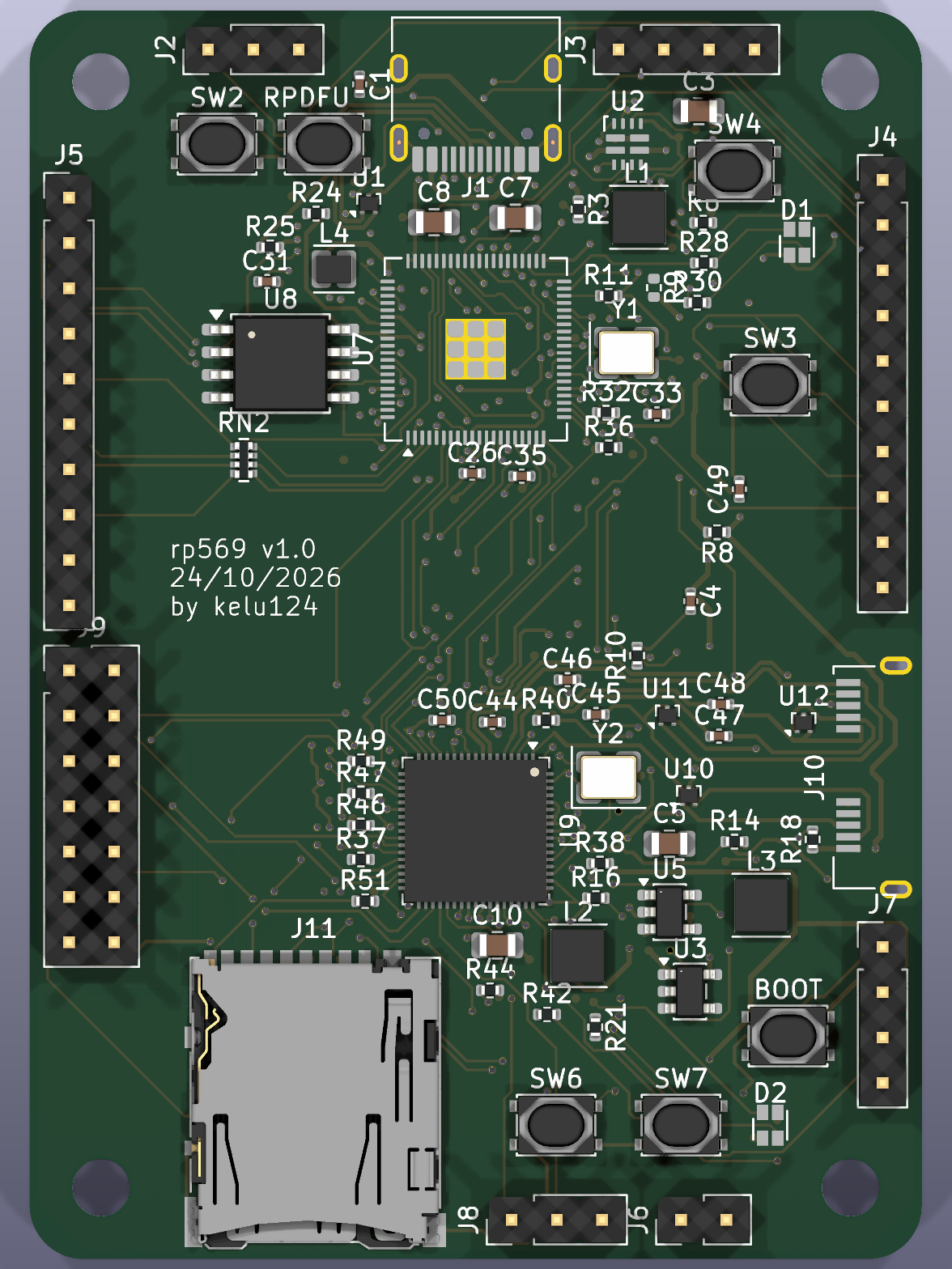
What is on the board
| Block | RP2350B side | CH569 side |
|---|---|---|
| USB | USB-C, USB 2.0 (firmware, debug, test control) | USB 3.0 Micro-B with through-hole shell legs |
| Storage | QSPI flash | microSD on the eMMC/SD controller (4-bit) |
| User I/O | RGB LED, 2 buttons, I2C header | RGB LED, 2 buttons, I2C header (bit-banged) |
| Expansion | 1x10 header (ADC0–5, debug UART) | 2x07 header, 12 GPIOs |
| Boot | BOOTSEL + RUN | BOOT button + jumper for a blank chip |
Between the chips: an 8-bit HSPI bus with clock and handshake lines, a shared I2C bus and a UART.
Why 8-bit and not 16-bit HSPI
The CH569’s HSPI can be 8, 16 or 32 bits wide, but its upper data lines share pins with the eMMC/SD controller. 16 bits would have cost the SD card, so the bus is 8 bits (HD0–HD7) plus the HSPI control lines. The RP2350 drives it from PIO: GPIO8–23 sit together on one side of the QFN, facing the CH569.
A logic analyser for free
Eight more RP2350 pins (GPIO0–7, consecutive for a PIO in pins, 8) come out on a 10-pin header with 100 Ω
series resistors. The plan: PIO samples them and the samples go down the HSPI bus to the CH569 and out over
USB 3. That turns the board into a simple streaming logic analyser, and gives the HSPI link a real workload.
The RP2350 is in charge of the CH569
This board is meant for automated tests, so the CH569 must never need a finger on a button:
- The CH569 is powered from its own USB3 VBUS through an AP2171W load switch that the RP2350 enables, so the RP2350 can power-cycle it.
- HSPI_D0 is also the CH569’s boot pin (PA5). Holding it low while the RP2350 turns the CH569 on puts the CH569 in its USB bootloader, exactly what the BOOT button does, so it can be reflashed from the host without touching the board. A 2-pin jumper does the same for a blank chip.
- The RP2350 also drives the CH569’s reset line and watches its 3.3 V rail and the USB3 VBUS through ADC pins.
The two USB inputs are combined by a TI TPS2121 power mux (with over-voltage dividers and a 1.2 A limit), so plugging both connectors never back-feeds one into the other.
Made to be made
The board is a 4-layer JLCPCB stack (JLC04161H-7628), 1.6 mm, parts on both sides, and every part carries an LCSC number so JLCPCB can assemble it. Two parts are not in JLCPCB’s catalogue and have to be consigned: the CH569W itself and the Amphenol USB3 Micro-B with through-hole legs (chosen because a USB3 Micro-B with only SMD pads is easy to rip off).
The whole KiCad project is generated from one Python file (hardware/gen/board.py: parts, footprints and a
pin-to-net map), which writes the schematic, the placed PCB and the net classes and runs ERC/DRC. The routing story
is in the next log.
Status
v1.0 is routed (0 unconnected, 0 DRC errors) and the JLCPCB production files are generated. Not ordered yet: the USB pairs still need re-routing as proper coupled pairs, and the silkscreen needs a clean-up. No firmware yet; the HSPI framing and the PIO transmitter are the next big pieces.
Sources, decisions and datasheet references: https://github.com/kelu124/rp569